Biasing a simple common-emitter amplifier using current mirrors
Using resistors to bias transistors limits the common emitter amplifier’s gain and the minimum supply voltage. This is due to the fact the the DC operating point and the small signal gain both depend on the value of the resistor, ![]() :
:
![]()
![]()
As we increase the gain by increasing ![]() , the voltage across
, the voltage across ![]() increases, and thus requires a higher supply voltage to maintain the same DC output voltage.
increases, and thus requires a higher supply voltage to maintain the same DC output voltage.
One way around this trade-off is to use current sources to bias the BJT, and one of the best ways to build a current source is to use a current mirror.
Consider the circuit below:
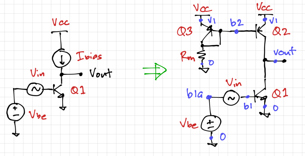
In this example, let us use the 2N3904 NPN BJT for Q1, and the 2N3906 PNP transistor for Q2 and Q3, and we need to bias transistor Q1 with ![]() , and set the amplifier output DC voltage to 2.5V with
, and set the amplifier output DC voltage to 2.5V with ![]() .
.
From our Mini-project 0 characterizations, we saw that:
| 2N3904 (NPN) | 2N3906 (PNP) | |
| 8.55e-12 | 1.25e-13 | |
| 1.40 | 1.20 | |
| 6.56 | 6.89 | |
| 135.63 | 241.53 |
Current Mirror Design
Since the target collector current of Q2 is ![]() , with
, with ![]() , we can plug this into the ideal BJT equation to find
, we can plug this into the ideal BJT equation to find ![]() :
:

We can then calculate the required collector current of Q3, ![]() as:
as:

And with ![]() and
and ![]() , we get:
, we get:
![]()
And the base currents, ![]() and
and ![]() :
:
![]()
![]()
Thus, we can solve for ![]() as:
as:
![]()
Using the ideal BJT equation, we can get ![]() :
:

Let’s write a netlist for the amplifier, with a DC sweep of the input voltage, Vin, and using the library file 2N390X.lib:
* Common Emitter Amplifier with Current Mirror Bias
* LPA 2020-04-16

.include 2N390X.lib
.options savecurrents

Vcc		v1 0		dc 5.0

* the pnp current mirror
Q2		vout b2 v1	2N3906
Q3		b2 b2 v1	2N3906

* the bias resistor
Rm		b2 0		5.277k

* the npn gain transistor
Q1		vout b1 0	2N3904

Vin 	b1 b1a		dc 0 sin(0 10m 1k)
Vbe1	b1a 0		dc 662.22m

.control

dc Vin -100m 100m 1m
wrdata amp_ce_cm_transfer_sim.dat v(vout) @Q1[ic]

alter Vbe1 dc = 666m
dc Vin -100m 100m 1m
wrdata amp_ce_cm_transfer_sim2.dat v(vout) @Q1[ic]

.endc

.end
Using this Python script, we can run the simulation, read in the results, and plot the transfer characteristics of the amplifier.
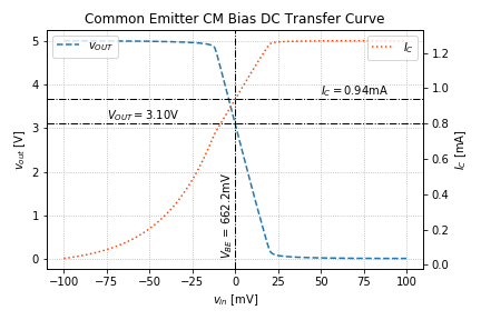
Notice that we are off by quite a bit, since the DC output voltage is at 3.1V and not at our desired level of 2.5V, and the collector current of Q2 is slightly less than 1mA.
From Figure 2, we can see that if we increase ![]() by a small amount, then the DC output voltage goes down, and the collector current increases. In SPICE, we can use the
by a small amount, then the DC output voltage goes down, and the collector current increases. In SPICE, we can use the alter command (line 27) to change the DC voltage of the source. Let’s increase Vbe1 to 666mV, and run the simulation again.
The results of the simulation is plotted below:
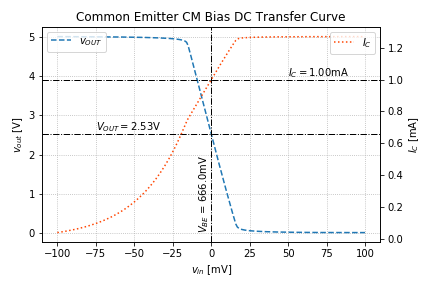
 by less than 4mV.
Notice that by changing ![]() by a very small amount (3.8mV) changes the bias or quiescent point of the amplifier by a relatively large amount. This is due to the exponential nature of the BJT’s transfer characteristics. This is also the reason we avoid using a voltage source to bias the base-emitter junction of the BJT.
by a very small amount (3.8mV) changes the bias or quiescent point of the amplifier by a relatively large amount. This is due to the exponential nature of the BJT’s transfer characteristics. This is also the reason we avoid using a voltage source to bias the base-emitter junction of the BJT.
If we plot the small signal gain by taking the derivative of the amplifier transfer characteristic in Figure 3, we get:
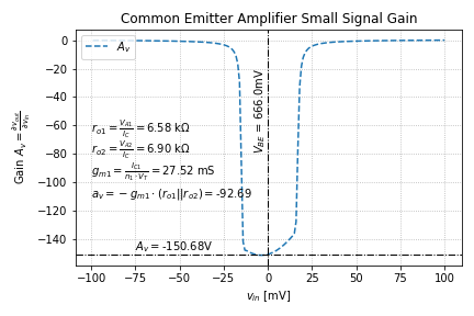
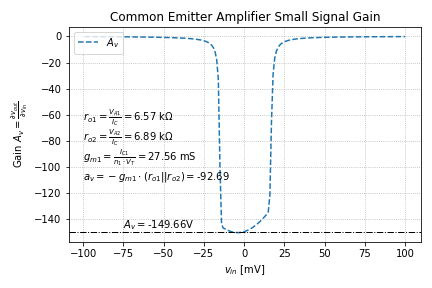
By using a current source, we can get away with larger output resistances, while maintaining the same supply voltage. Also notice that we get a relatively large discrepancy in predicted versus simulated gain due to the fact the we derived our ideal BJT parameters using the transfer, input, and output characteristics, but we did not fit it to their derivatives. Thus, we expect our prediction of the small signal parameters to be less accurate. However, in our case, this is acceptable, and we will show why this is so in the tutorials leading up to feedback amplifiers.
Input Biasing
A better biasing strategy is to, once again, generate ![]() using a diode connected transistor, as shown below:
using a diode connected transistor, as shown below:
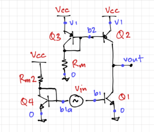
Q1 with a diode-connected transistor Q4.The diode-connected transistor Q4 is added to generate the ![]() needed by
needed by Q1. We can calculate the value of Rm2 using the same methodology we used to calculate Rm, giving us
![]()
Note that the input voltage source is in an awkward position, with no terminal connected to ground. Ignore this for now and we’ll bet back to this issue when we talk about differential amplifiers. Also note that in using current mirrors, the only DC voltage source we have left is Vcc.
We will use this netlist to simulate the circuit in Figure 4:
* Common Emitter Amplifier with Current Mirror Bias
* LPA 2020-04-16

.include 2N390X.lib
.options savecurrents

Vcc		v1	0		dc 5.0

* the pnp current mirror
Q2		vout b2 v1	2N3906
Q3		b2 b2 v1	2N3906

* the bias resistor
Rm		b2 0		5.277k
* Rm		b2 0		5.1k

* the npn gain transistor
Q1		vout b1 0	2N3904

Vin 		b1 b1a		dc 0 sin(0 10m 1k)

* the npn current mirror
Q4		b1a b1a 0	2N3904
Rm2		v1 b1a		5.352k
* Rm2		v1 b1a		5.1k

.control

dc Vin -100m 100m 1m
wrdata amp_ce_cm2_transfer_sim.dat v(vout) @Q1[ic]

tran 1u 5m
wrdata amp_ce_cm2_transient_sim.dat v(vout) v(b1)

.endc

.end
Using this Python script to run the simulation and plot the results, we get
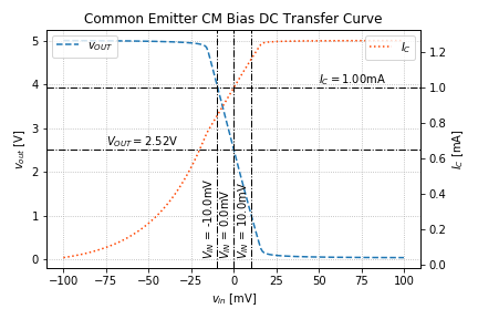
As we can see from Figure 5, our DC bias is almost spot-on. In fact, the bias is very stable even if we change the values of the two resistors to the closest standard value. In this case, ![]() . You can try this be commenting out lines 14 and 24, and uncommenting lines 15 and 25. This is due to the linear relationship between the resistors and the collector currents, instead of the exponential dependence of the collector current to the base-emitter voltage.
. You can try this be commenting out lines 14 and 24, and uncommenting lines 15 and 25. This is due to the linear relationship between the resistors and the collector currents, instead of the exponential dependence of the collector current to the base-emitter voltage.
Taking the derivative of the transfer curve in Figure 5, we get the small signal gain plot:
We can also plot the transient response:
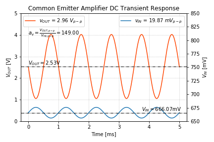
Note that the output swing is from approximately 1V to 4V, as predicted by Figure 5 for a 20mV peak-to-peak input. Also note that the transistor Q4 calculated the required ![]() correctly.
correctly.
End of Tutorial 5
Congratulations! You have just biased a common emitter amplifier using current mirrors.
