Differential Amplifiers
Differential amplifiers gives us, among other things, (1) the capability to reject common-mode signals, (2) increased signal swing, and (3) a wide common-mode input range, making it easier to cascade amplifiers. However, this comes at a price: a (more than) doubling of the number of (1) circuit elements and (2) power consumption.
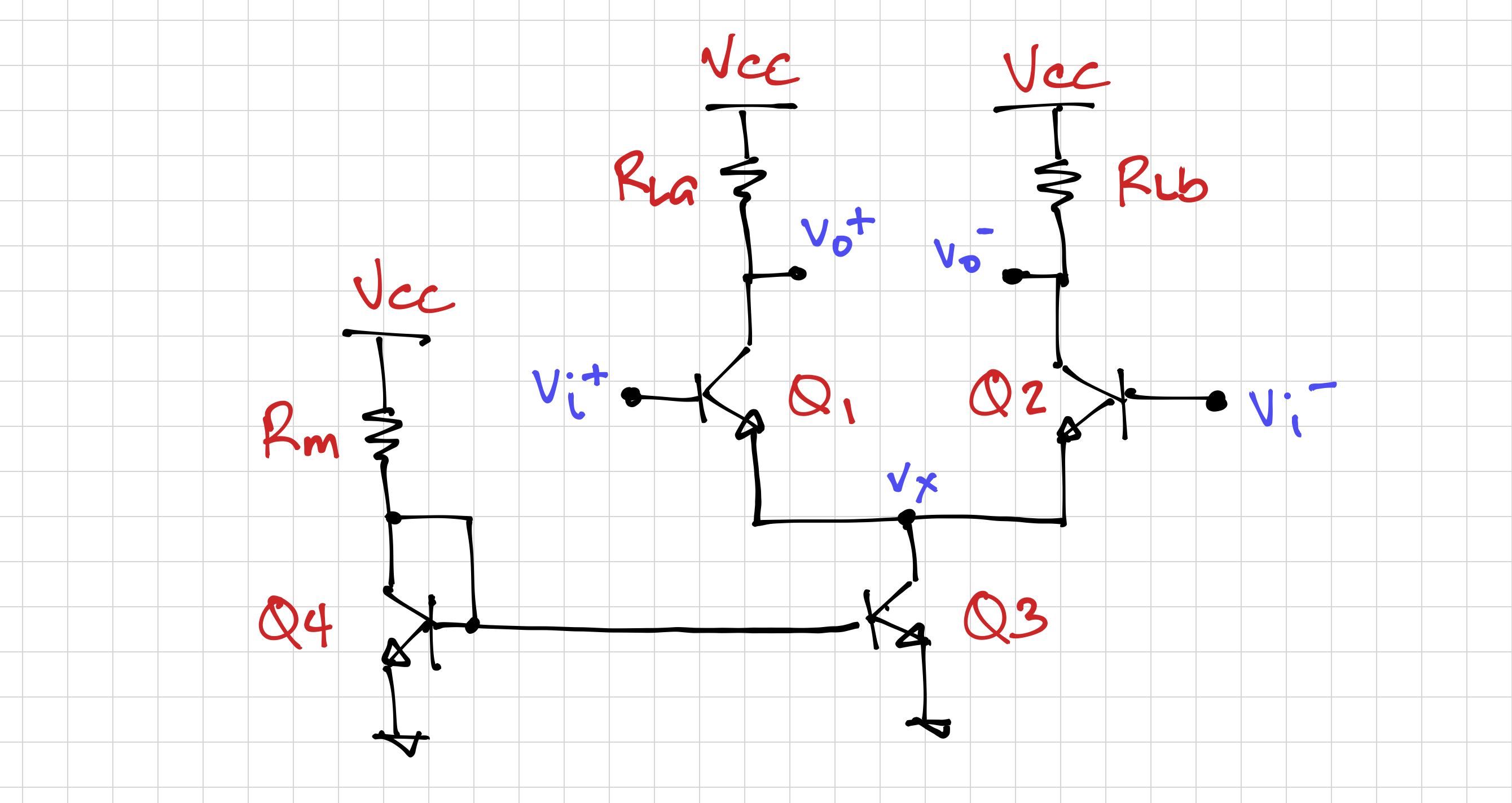
Figure 1 shows the basic differential amplifier, composed of (1) the emitter-coupled pair, Q1 and Q2, (2) the tail current source, Q3, and (3) the load resistors ![]() .
.
Biasing the Differential Amplifier
Once again, let us (arbitrarily) set the DC collector currents of transistors Q1 and Q2 to 1mA. Thus, the tail current source, and hence ![]() , should be equal to 2mA.
, should be equal to 2mA.
We know that ![]() follows the common-mode input, and that the minimum
follows the common-mode input, and that the minimum ![]() should be large enough to keep
should be large enough to keep Q3 in the forward-active region:
![]()
Let us set ![]() to leave some margin that we could potentially exploit later. From
to leave some margin that we could potentially exploit later. From ![]() , we can calculate
, we can calculate ![]() :
:
![]()
From ![]() , we can also calculate the minimum output swing of the positive output,
, we can also calculate the minimum output swing of the positive output, ![]() :
:
![]()
Note that if we use ![]() in the equation above, we will not get any leeway in choosing the input common-mode, which is synonymous to the DC voltage at the input of the differential amplifier. If we choose
in the equation above, we will not get any leeway in choosing the input common-mode, which is synonymous to the DC voltage at the input of the differential amplifier. If we choose ![]() , then we can calculate the maximum input common-mode voltage:
, then we can calculate the maximum input common-mode voltage:
![]()
This gives us a relatively large common-mode input range (CMIR):
![]()
Note that ![]() . Therefore, for a
. Therefore, for a ![]() , the output swing of
, the output swing of ![]() (and
(and ![]() as well) is
as well) is
![]()
If we want to bias the output at the middle of this range, i.e. when ![]() (the quiescent collector current of
(the quiescent collector current of Q1), we need a load resistance of
![]()
To bias our tail current source transistor, Q3, we once again use our procedure in tutorial 5, with ![]() , and choosing
, and choosing ![]() to be at the midpoint of
to be at the midpoint of ![]() and
and ![]() . Thus, with
. Thus, with ![]() , we get
, we get
![]()
Small Signal Gain
Recall that for the differential amplifier in Figure 1, the differential mode gain, ![]() , is given by
, is given by
![]()
And the common-mode gain, ![]() , is given by
, is given by
![]()
To achieve a reasonable amount of common-mode rejection, we want ![]() . One convenient way to increase the output resistance of the tail current source is to degenerate the current mirror using
. One convenient way to increase the output resistance of the tail current source is to degenerate the current mirror using ![]() , as seen in Figure 2.
, as seen in Figure 2.
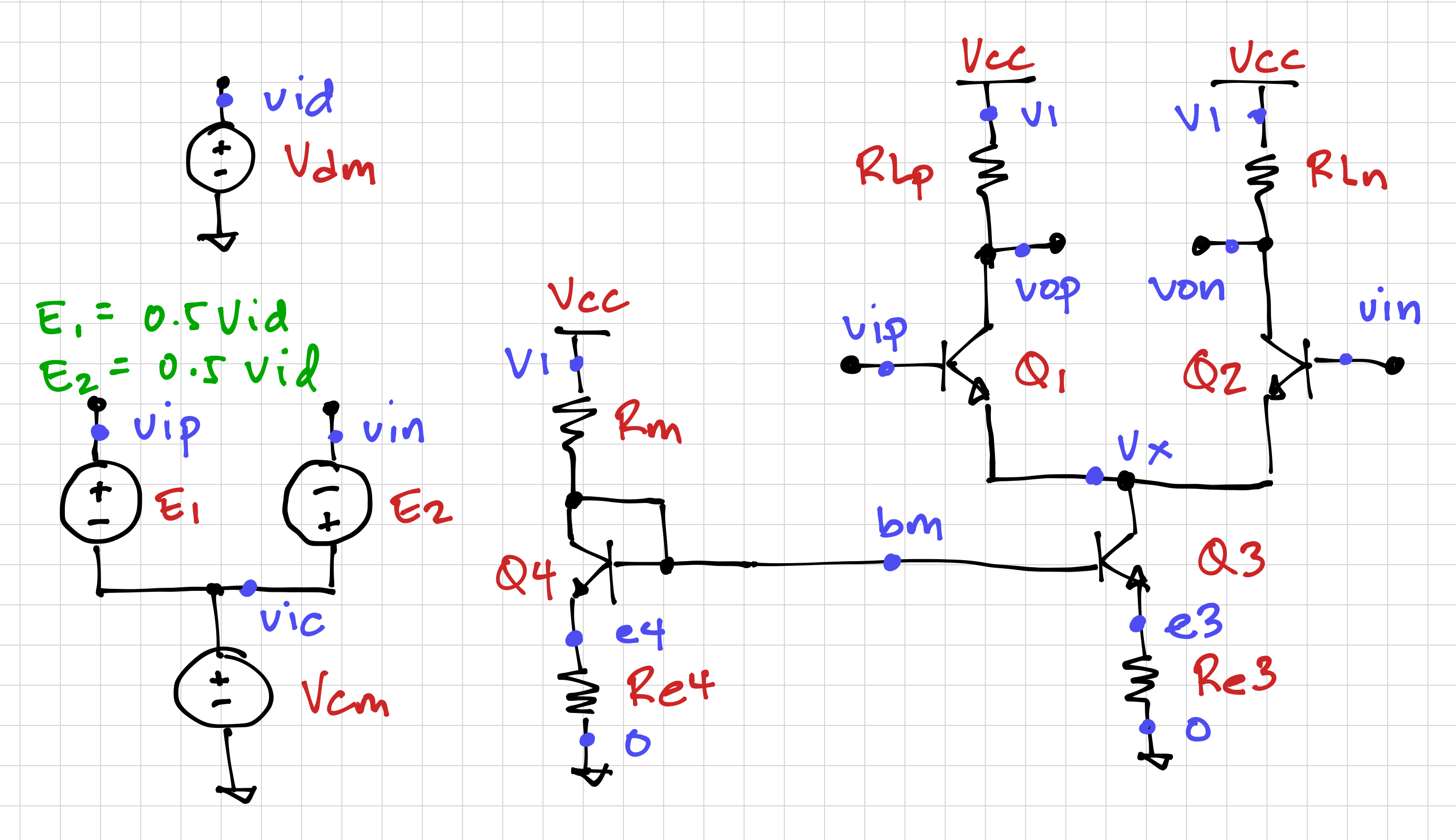
The output resistance of the degenerated current mirror in Figure 2 can then be calculated (from its small signal model) as
![]()
This increased output resistance comes as a cost, an increase in the minimum required voltage across the current source:
![]()
Since we added a margin of 300mV to ![]() earlier, for
earlier, for ![]() , we can accommodate, at most, a degeneration resistance of
, we can accommodate, at most, a degeneration resistance of ![]() . Note that you have to maintain the same bias current, you have to subtract the voltage across
. Note that you have to maintain the same bias current, you have to subtract the voltage across ![]() when computing for
when computing for ![]() .
.
Simulating the Differential Amplifier
Let’s use simulate our differential amplifier using this netlist, with current sources using degeneration resistances, ![]() , and using this Python script to examine our results. Note the use of voltage-controlled voltage sources to generate
, and using this Python script to examine our results. Note the use of voltage-controlled voltage sources to generate ![]() and
and ![]() from
from ![]() and
and ![]() .
.
Looking at our tail current source, let’s plot the tail current as we vary the input common mode:
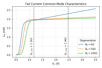
Notice that without degeneration, ![]() is relatively small, resulting in a large tail current variation as we change
is relatively small, resulting in a large tail current variation as we change ![]() . Also note the larger
. Also note the larger ![]() values as we increase
values as we increase ![]() .
.
Let’s use ![]() in our succeeding simulations to keep the tail current as flat as possible over the CMIR without sacrificing our output swing.
in our succeeding simulations to keep the tail current as flat as possible over the CMIR without sacrificing our output swing.
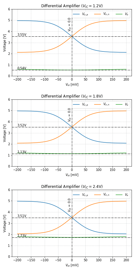
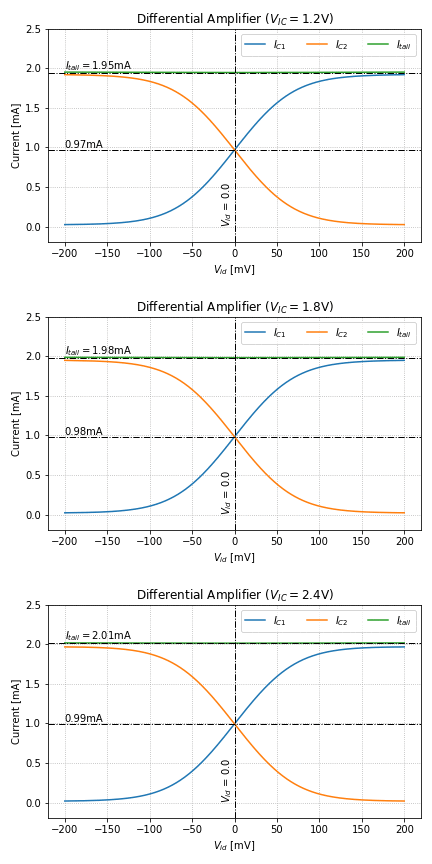
Figure 4 shows the behavior of the output nodes and ![]() as we vary
as we vary ![]() , for a
, for a ![]() of 1.2V, 1.8V, and 2.4V. The behavior of the currents, on the other hand, are shown in Figure 5.
of 1.2V, 1.8V, and 2.4V. The behavior of the currents, on the other hand, are shown in Figure 5.
 as we vary
  , for a different values of
  .
.
 , for a different values of
  .
.Looking at the behavior of ![]() in Figure 4, we see that it is relatively constant as
in Figure 4, we see that it is relatively constant as ![]() is varied, hence, it can be considered a “virtual ground” in small-signal analysis. We can also see that even for
is varied, hence, it can be considered a “virtual ground” in small-signal analysis. We can also see that even for ![]() ,
, ![]() (and
(and ![]() ) is still greater than
) is still greater than ![]() by at least a
by at least a ![]() , keeping
, keeping Q1 (and Q2) in the forward-active region at all times.
Figure 6 shows the differential transfer characteristics of the amplifier, where ![]() . Note that the common-mode voltage has very little effect on the transfer characteristics, and that the differential output swing is twice that of the single-ended outputs.
. Note that the common-mode voltage has very little effect on the transfer characteristics, and that the differential output swing is twice that of the single-ended outputs.
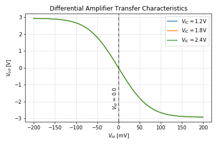
Taking the derivative of the transfer curves in Figure 6, we get the differential mode gain plots in Figure 7.
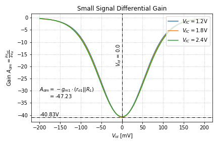
We can see that the simulated differential mode gain agrees with the gain obtained using half-circuit analysis.
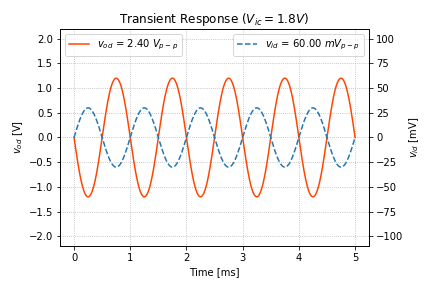
Figure 8 shows the differential transient response of the amplifier, and note that (1) the differential output is zero when the differential input is zero, and (2) the swing is bipolar, i.e. goes from +1.2V to -1.2V, and can potentially be larger than the supply voltage.
End of Tutorial 7
Congratulations! You have just biased a differential amplifier, increased the output resistance of its tail current, and simulated the effects of the differential- and common-mode inputs on the behavior of key differential amplifier voltages and currents.
