A Simple Three-Stage Operational Amplifier
Operational amplifiers (op-amps) are one of the most commonly used analog circuit building blocks due to its high gain, differential input, and low output impedance. We can build a simple op-amp using (1) a differential amplifier, for the differential input, (2) a common-emitter amplifier, for gain, and (3) a common-collector amplifier as the last stage, for its low output impedance.
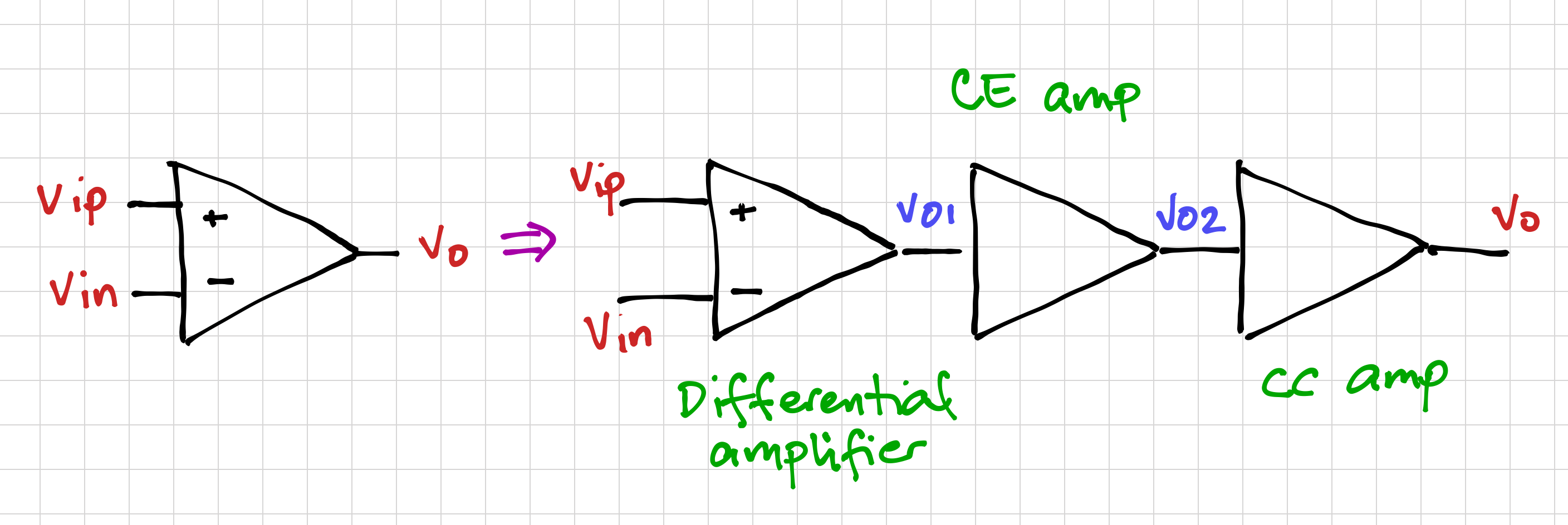
To get an idea of the individual amplifier voltage swings, if we set the op-amp output swing of 3V, and a common-emitter amplifier with a gain of 100, the output swing of the differential amplifier will be around 30mV. For a differential amplifier gain of around 40, we expect an input swing of about 750![]() A.
A.
The Single-Ended Output Differential Amplifier
Since we need a differential amplifier with a single-ended output, we can use a current mirror load to efficiently convert the differential output current to a single-ended output voltage. However, one drawback of the BJT current mirror is the inherent mismatch between the two collector currents due to their associated base currents. In a differential amplifier, where matching is crucial, this inherent mismatch can cause significant performance degradation, such as increased input offset voltages.
We can reduce the effect of the base currents by adding another transistor, Q3, to provide the base current required, while still ensuring that transistor Q2 remains in the forward active region.
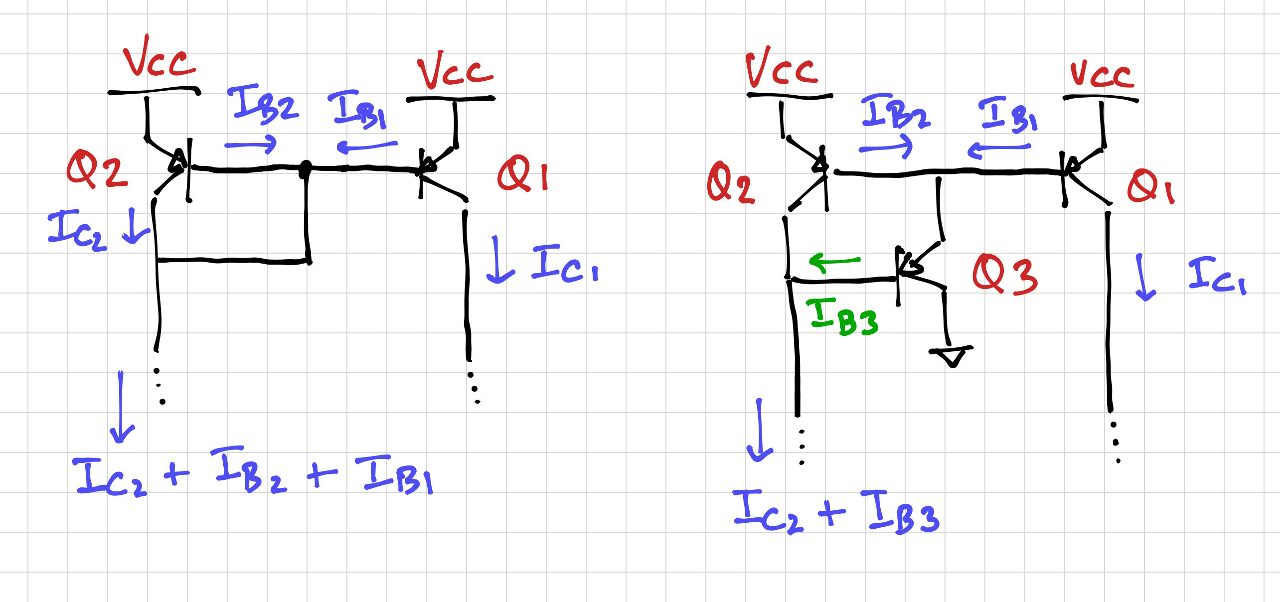
Q3 to reduce the errors due to the base currents of Q1 and Q2.Notice that instead of ![]() , we can reduce the error by a factor of
, we can reduce the error by a factor of ![]() :
:
![]()
Note that if we assume that ![]() is negligible, and if we further assume
is negligible, and if we further assume ![]() to be equal to
to be equal to ![]() , then
, then ![]() .
.
Using small signal analysis, we can show that the modified current mirror is still a small signal current mirror. That is, a small signal input current will produce a small signal mirrored output current. It is this small signal current mirroring that enables us to maintain the differential amplifier’s effective transconductance even when the output is single-ended.
We can now use this modified current mirror load to build our single-ended output differential amplifier:
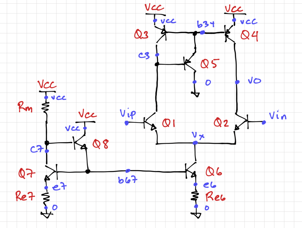
Notice that we are also using the modified current mirror as our tail current. This simplifies our calculation of the bias resistor ![]() , and at the same time, if we set our nominal input common-mode voltage,
, and at the same time, if we set our nominal input common-mode voltage, ![]() to 1.8V (we’ll revisit this later), then the
to 1.8V (we’ll revisit this later), then the ![]() of
of Q6 and Q7 will be closer to each other.
Since this amplifier will be part of a larger circuit, it is convenient to create a subcircuit for this since (1) it will be easy to ‘instantiate’ a number of these amplifiers if necessary, and (2) we will not have to keep track of our node and device numbering, since these will be local to the subcircuit. Thus, we can describe our amplifier using this netlist:
**************************************************
* differential input single-ended output amplifier
.subckt diffamp_n vip vin vo vcc

* input pair
Q1		c3 vip vx		2N3904
Q2		vo vin vx		2N3904

* current mirror load
Q3		c3 b34 vcc		2N3906
Q4		vo b34 vcc		2N3906
Q5		0 c3 b34		2N3906

* tail current source
Q6		vx b67 e6		2N3904
Q7		c7 b67 e7		2N3904
Q8		vcc c7 b67		2N3904

* tail current degeneration
Re6		e6 0 			100
Re7		e7 0 			100

* bias resistor
Rm		vcc c7			{Rmdiff}

.ends diffamp_n
We can then include this file into our main SPICE netlist. The subcircuit begins with the .subckt command, followed by the subcircuit name, and the subcircuit’s interface pins or nodes. The circuit description follows, and concludes with the .ends command. Note that the value of resistor Rm is a parameter, Rmdiff. It is enclosed in curly braces, and can be defined in the man netlist.
If we use a tail current of 2mA, we can use a simple Python script to numerically calculate the emitter-base voltage of Q3. Noting that ![]() and iterating over the following equations until
and iterating over the following equations until ![]() , starting with a reasonable guess for
, starting with a reasonable guess for ![]() :
:


We get ![]() . From this, we can calculate
. From this, we can calculate ![]() . And using
. And using ![]() , using the ideal BJT equation, we can calculate
, using the ideal BJT equation, we can calculate ![]() . Thus, the DC output voltage of the differential amplifier is
. Thus, the DC output voltage of the differential amplifier is
![]()
Note that this is higher than ![]() , but since (1) the output swing we expect is relatively small (less than 50mV), and (2) the input DC voltage of a common-emitter amplifier is either close to
, but since (1) the output swing we expect is relatively small (less than 50mV), and (2) the input DC voltage of a common-emitter amplifier is either close to ![]() (PNP BJT) or close to ground (NPN BJT), this is perfectly acceptable.
(PNP BJT) or close to ground (NPN BJT), this is perfectly acceptable.
Similarly, we can iterate over the next two equations to find ![]() :
:

![]()
This gives us ![]() . And using
. And using ![]() and
and ![]() , we can get
, we can get ![]() , then
, then ![]() , then
, then ![]() , and eventually
, and eventually ![]() . This then leads to the value of our bias resistor,
. This then leads to the value of our bias resistor, ![]() :
:
![]()
We can then estimate the small signal parameters of the differential amplifier:
![]()
![]()
The Common-Emitter Stage
Since the DC output voltage of the differential amplifier is closer to ![]() , it is convenient to use a PNP common-emitter amplifier, like the one shown below:
, it is convenient to use a PNP common-emitter amplifier, like the one shown below:
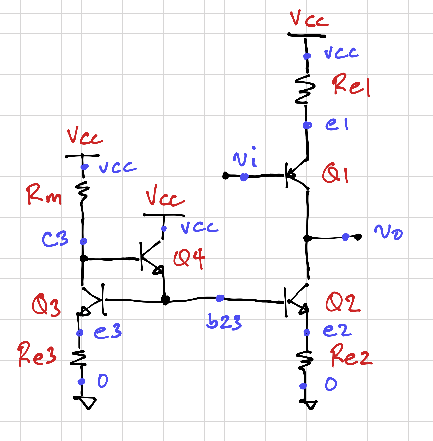
Since the differential output voltage is approximately two ![]() drops below
drops below ![]() , we can use the degeneration resistor
, we can use the degeneration resistor Re1 (1) to absorb the one of these ![]() drops, (2) to increase the input impedance of the common-emitter amplifier, and (3) to increase the common-emitter gain by increasing its output impedance, but with reduced effective transconductance and output swing. In order to take full advantage of the increased output impedance looking into the collector of
drops, (2) to increase the input impedance of the common-emitter amplifier, and (3) to increase the common-emitter gain by increasing its output impedance, but with reduced effective transconductance and output swing. In order to take full advantage of the increased output impedance looking into the collector of Q1, we also degenerate Q2 (and Q3 as well for easier biasing).
The SPICE netlist for our common-emitter amplifier subcircuit is shown below:
******************************
* pnp common emitter amplifier
.subckt ceamp_p vi vo vcc

* gm (gain) transistor
Q1		vo vi e1		2N3906
Re1		e1 vcc			{Repce}

* current mirror load
Q2		vo b23 e2		2N3904
Q3		c3 b23 e3		2N3904
Q4		vcc c3 b23		2N3904

Re2		e2 0 			{Rence}
Re3		e3 0 			{Rence}

Rm		vcc c3			{Rmce}

.ends ceamp_p
To calculate the value of Re1 such that we get ![]() ,
, ![]() (more on this later as well), and with the input DC voltage equal to the differential amplifier’s output DC voltage, we can iterate over the following equations:
(more on this later as well), and with the input DC voltage equal to the differential amplifier’s output DC voltage, we can iterate over the following equations:

![]()
We then get ![]() . We can calculate
. We can calculate ![]() by equating the small signal impedances looking into the collector of
by equating the small signal impedances looking into the collector of Q1 and into the collector of Q:
![]()
Thus, ![]() .
.
Similar to our calculation of the bias resistor of the differential amplifier tail current, we then get ![]() .
.
Calculating the small signal parameters of the common-emitter amplifier, we get:
![]()
![]()
![]()
![]()
The Common-Collector Output Stage
The last stage of our three-stage operational amplifier is the common-collector amplifier, shown below.
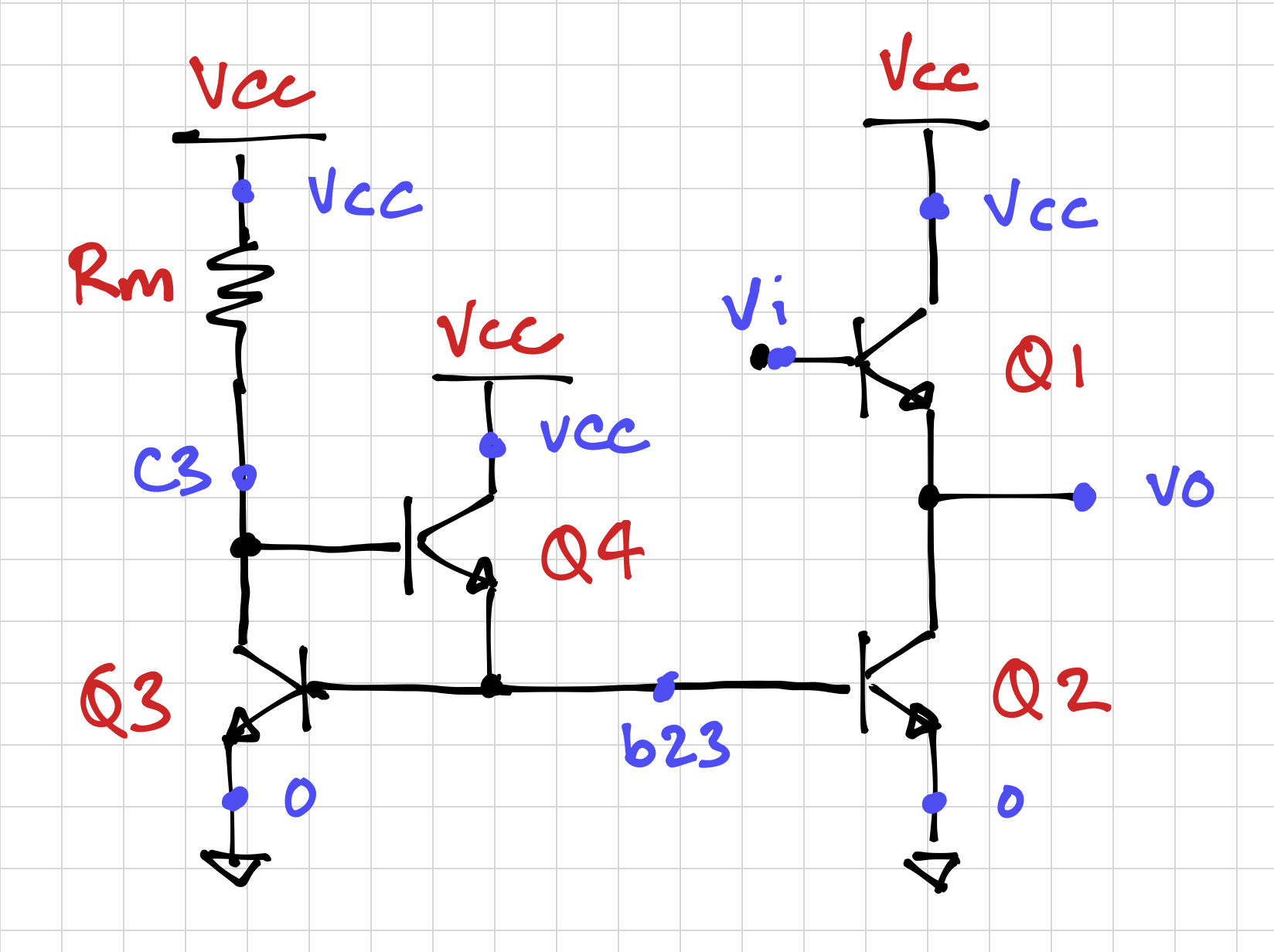
Since operational amplifiers are commonly used in feedback circuits, it is advantageous to set the output DC voltage within the input common-mode range of the op-amp. In this case, let us set the output DC voltage equal to the common-mode input voltage of 1.8V. This way, for example, we can connect the output node to the negative input (vin) and still maintain our circuit bias conditions.
Also notice that the input DC voltage of the NPN common-collector stage will always be higher than the output DC voltage by ![]() . The opposite is true if we were to use a PNP common-collector stage. Thus, by setting the output DC voltage of the common-emitter stage to 2.5V, we can set the output DC voltage of the common-collector stage to around 1.8V if
. The opposite is true if we were to use a PNP common-collector stage. Thus, by setting the output DC voltage of the common-emitter stage to 2.5V, we can set the output DC voltage of the common-collector stage to around 1.8V if ![]() .
.
The SPICE netlist below describes the common-collector amplifier subcircuit:
*************************************
* npn output stage (common collector)
.subckt ccamp_n vi vo vcc

Q1		vcc vi vo		2N3904

* current mirror bias
Q2		vo b23 0		2N3904
Q3		c3 b23 0		2N3904
Q4		vcc c3 b23		2N3904

Rm		vcc c3			{Rmcc}

.ends ccamp_n
Again, if we arbitrarily set the bias current to 1mA, we can calculate the ![]() needed to generate 1mA, with a
needed to generate 1mA, with a ![]() :
:

We can then calculate ![]() :
:

Thus, the bias resistor, ![]() can be calculated as
can be calculated as
![]()
Calculating the small signal parameters of the common-collector amplifier, we get:
![]()
![]()
![]()
Putting It All Together
Let’s build our three-stage operational amplifier by instantiating our three component amplifiers using the SPICE netlist below:
* A simple 3-stage opamp
* LPA 2020-04-16

.include 2N390X.lib
.options savecurrents

.include diffamp_n.sp
.include ceamp_p.sp
.include ccamp_n.sp

* calculated values
.param Rmdiff = 1.788k Rmce = 3.161k Rmcc = 3.823k Repce = 545 Rence = 672

* instantiate the 3 amplifiers
X1		vip vin vo1 vcc		diffamp_n
X2		vo1 vo2 vcc			ceamp_p
X3		vo2 vo3 vcc			ccamp_n

* supply voltage
V1		vcc 0 			5.0

* voltage controlled voltage sources to generate vip and vin from vid
E1		vip vic vid 0	0.5
E2		vic vin vid 0	0.5

* differential input
Vdm 	vid 0		dc 0 sin(0 100u 1k)

* common mode input
Vcm		vic 0		dc 1.8
In SPICE, we can instruct the simulator to include the files that contain our component amplifiers, as seen in lines 7-9. Subcircuits are instantiated using the ‘X‘ identifier as shown in lines 15-16, with the corresponding interface nodes, and the subcircuit name. The node order corresponds to our node order when defining the subcircuit.
Line 12 provides the values for the global parameters we have defined in the subcircuits. This makes it easy for us to tweak all our design values in the top-level SPICE file, without having to open the subcircuit files.
Simulating the Three-Stage Operational Amplifier
A good way to make sure our netlist is written correctly is to check the bias conditions of our amplifiers. To do this, we can run an operating point analysis within the control block, as shown below:
.control

* let's check the DC voltages and currents using the DC operating point (op) analysis
op
print @Q.X1.Q1[ic] @Q.X1.Q2[ic] @Q.X1.Q6[ic]
print @Q.X2.Q1[ic] @Q.X2.Q2[ic]
print @Q.X3.Q1[ic] @Q.X3.Q2[ic]
print v(vo1) v(vo2) v(vo3)

.endc

.end
Note the format for printing the currents of a transistor inside a subcircuit, and we can once again see that the simulator can discriminate between transistor Q1 in subcircuit X1 (the differential amplifier) and the transistor Q1 in subcircuit X2 (the common-emitter amplifier). After running the simulation, we will get this report:
******
** ngspice-31 : Circuit level simulation program
** The U. C. Berkeley CAD Group
** Copyright 1985-1994, Regents of the University of California.
** Please get your ngspice manual from http://ngspice.sourceforge.net/docs.html
** Please file your bug-reports at http://ngspice.sourceforge.net/bugrep.html
******
ngspice 1 -> source opamp1.sp

Circuit: * a simple 3-stage opamp

Doing analysis at TEMP = 27.000000 and TNOM = 27.000000


No. of Data Rows : 1
@q.x1.q1[ic] = 9.788230e-04
@q.x1.q2[ic] = 9.807522e-04
@q.x1.q6[ic] = 1.973474e-03
@q.x2.q1[ic] = 9.955196e-04
@q.x2.q2[ic] = 9.887787e-04
@q.x3.q1[ic] = 1.027488e-03
@q.x3.q2[ic] = 1.034229e-03
v(vo1) = 3.757409e+00
v(vo2) = 2.212725e+00
v(vo3) = 1.548787e+00
ngspice 2 ->
The bias currents and voltages are consistent with what we want, though the differential amplifier bias currents are slightly lower than 1mA, resulting in a slightly higher ![]() , which means a smaller
, which means a smaller ![]() for the input transistor of the common-emitter stage, resulting in a lower output voltage of the common-emitter amplifier, and hence the common-collector amplifier. Once again, we can see the disadvantage of biasing a relatively complex circuit without using feedback. We’ll revisit this biasing problem in our tutorial on feedback circuits.
for the input transistor of the common-emitter stage, resulting in a lower output voltage of the common-emitter amplifier, and hence the common-collector amplifier. Once again, we can see the disadvantage of biasing a relatively complex circuit without using feedback. We’ll revisit this biasing problem in our tutorial on feedback circuits.
Let’s increase the differential amplifier bias current by reducing the value of its ![]() to
to ![]() . This small adjustment results in:
. This small adjustment results in:
******
** ngspice-31 : Circuit level simulation program
** The U. C. Berkeley CAD Group
** Copyright 1985-1994, Regents of the University of California.
** Please get your ngspice manual from http://ngspice.sourceforge.net/docs.html
** Please file your bug-reports at http://ngspice.sourceforge.net/bugrep.html
******
ngspice 1 -> source opamp1.sp

Circuit: * a simple 3-stage opamp

Doing analysis at TEMP = 27.000000 and TNOM = 27.000000


No. of Data Rows : 1
@q.x1.q1[ic] = 1.013752e-03
@q.x1.q2[ic] = 1.015735e-03
@q.x1.q6[ic] = 2.043759e-03
@q.x2.q1[ic] = 9.974500e-04
@q.x2.q2[ic] = 9.904111e-04
@q.x3.q1[ic] = 1.060227e-03
@q.x3.q2[ic] = 1.067266e-03
v(vo1) = 3.755377e+00
v(vo2) = 2.472779e+00
v(vo3) = 1.807095e+00
ngspice 2 ->
Now the DC voltages and currents are very near our desired values. Let us plot the behavior of the amplifier outputs as we vary the input differential voltage using this Python script.
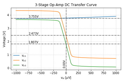
As expected, we have a relatively small gain from the differential amplifier. Most of the gain is from the common-emitter amplifier, and the common-collector stage has a gain of around unity, and shifts the DC voltage by a ![]() .
.
Looking at the overall transfer characteristics, we see that the output swing is around 2.79V for an input of 200![]() V peak-to-peak.
V peak-to-peak.
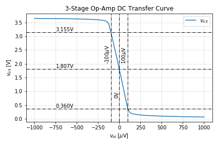
We can verify this via a transient simulation, the results of which are shown below:
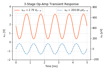
From Figure 8, we can see that the op-amp gain is approximately -13795. If we use our small signal calculations, we get
![]()
Notice that we just neglected the effect of loading since the input impedances are significantly larger than the output impedances at the amplifier interfaces. In cases where this is not true, you have to add the loading (voltage divider) terms. Once again, we can see the limitations of our models in estimating the small signal parameters. Note that by using feedback (later on), most of the time, we really do not need to accurately predict the small signal behavior. We usually just need to be better than a certain parameter.
End of Tutorial 8
Congratulations! You have just constructed and biased a simple 3-stage operational amplifier using a differential amplifier, a common-emitter amplifier, and a common-collector amplifier.
