A Trans-Impedance Amplifier (TIA)
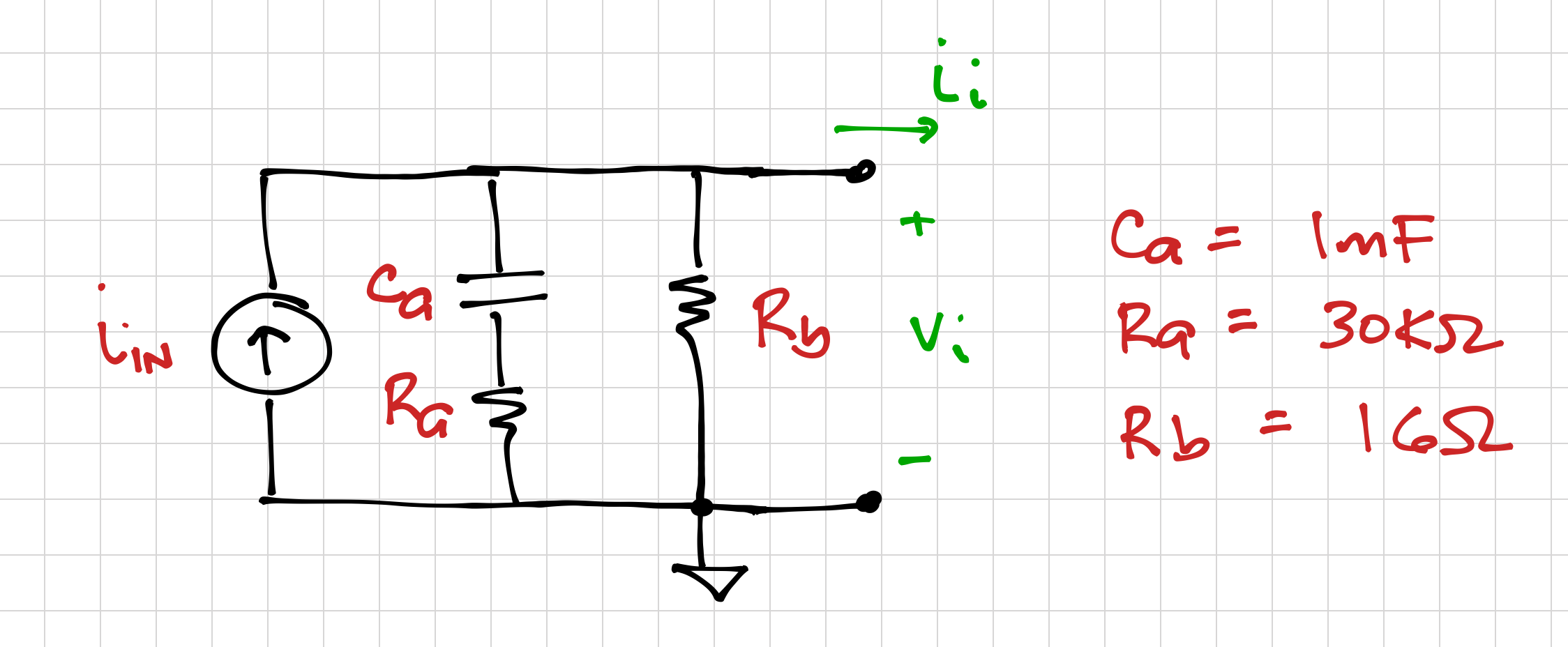
A common scenario in wired sensor systems is shown below. A sensor, in this case, a piezoelectric sensor, produces a small current when it detects small vibrations in a structure, for example a building or a staircase. The sensor output is then amplified by a trans-impedance amplifier, and sent to a central management unit via a 50-ohm coaxial cable.

To amplify this small current signal, we need an amplifier with a very small input resistance and, to drive a 50-ohm transmission line, the amplifier should also have a very small output impedance.
The output of a trans-impedance (TIA) amplifier is a voltage, and its input is a current. Thus, trans-impedance, or ‘gain’ is
![]()
A TIA can be built using a common-base amplifier as its input stage, a common-emitter amplifier as its gain stage, and a common-collector amplifier as its output stage:

The Common-Base Amplifier
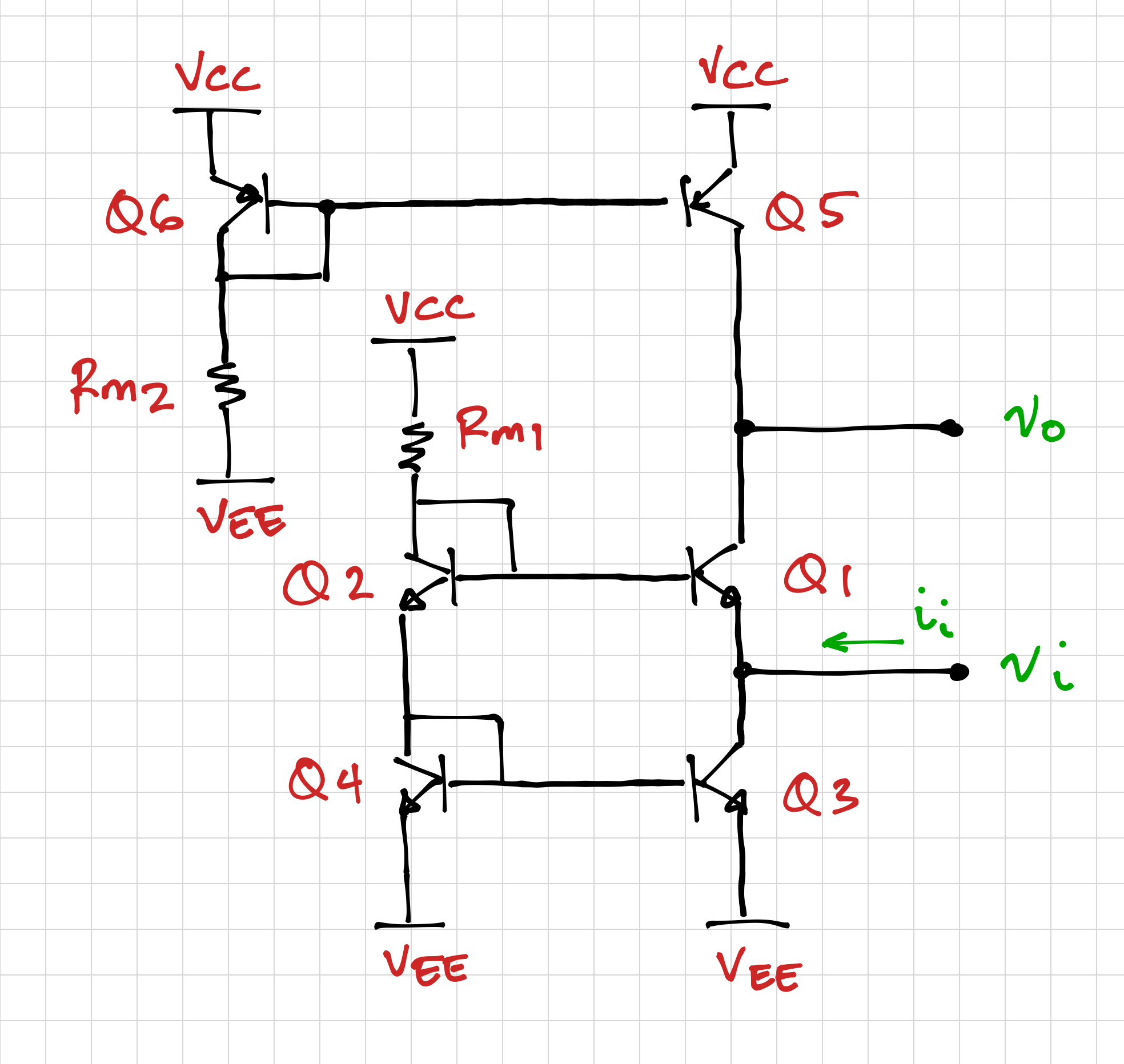
A simple common-base amplifier with its own bias circuit is shown below. Notice that the bias circuit provides the necessary collector current, as well as the corresponding ![]() and
and ![]() needed to keep all the transistors in the forward-active region.
needed to keep all the transistors in the forward-active region.

The input current is injected into the emitter of Q1, and the output voltage is taken at its collector. Make sure you understand why this is a common-base amplifier, and why a common-base amplifier is a good choice when the input is a current.
The TIA Specifications
In this mini-project, you are tasked to design a TIA using the 2N3904 and 2N3906 transistors, that can accept small-signal current input from a piezoelectric vibration sensor, modeled as

 ,
,  , and
, and  .
.The TIA is required to drive a 50-ohm transmission line at its output, with a peak-to-peak voltage of at least 400mV without clipping, for an input peak-to-peak current of 2![]() A at the small-signal current source,
A at the small-signal current source, ![]() .
.
Also, to avoid static current at the output, i.e. the output DC voltage is 0V, your amplifier will be powered using two supplies, a +2.5V supply, and a -2.5V supply.
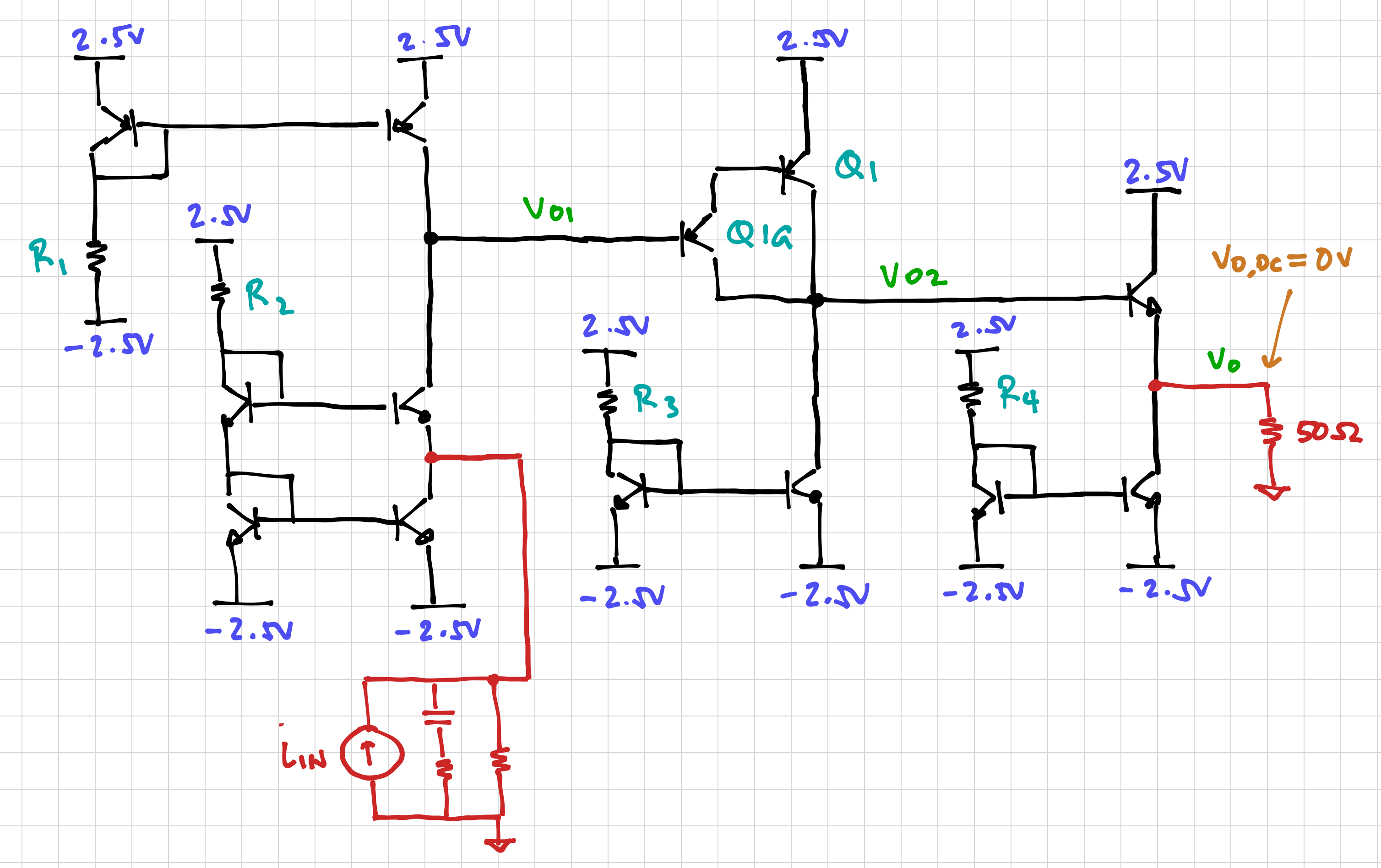
One possible implementation of a TIA is shown below. Note that the common-emitter amplifier uses a Darlington Pair, Q1 and Q1a, to reduce the impact of its input current on the bias of the common-base stage. Make sure you understand the implications of using a Darlington Pair instead of just a single transistor.

Make sure you understand why a PNP common-emitter amplifier is used instead of an NPN common-emitter amplifier.
Note that the circuit above is just a suggestion that can serve as a starting point since we encourage you to explore other topologies. Thus, your design is not limited to this particular biasing topology or TIA architecture.
Since most of these sensor systems are battery powered, you want to minimize the DC power consumed by your TIA, i.e, what is the smallest set of bias currents that can satisfy the specifications?
| Summary of TIA Specifications: | |
| Positive Supply Voltage | 2.5V |
| Negative Supply Voltage | -2.5V |
| Output DC Voltage | 0V |
| Output Load | 50 |
| Output voltage swing (@ | 400mV peak-to-peak |
| DC Power Consumption | Minimize |
What To Submit:
- A short 2-page writeup of your methodology including:
- An explanation of how you chose your topology, transistor bias currents and the inter-stage DC output voltages (
 and
and  ) within the TIA, together with the calculations used to determine the values of biasing resistors.
- The schematic of your TIA. (not included in the 2-page limit)
- A list of the target and simulated transistor bias currents and amplifier output voltages. (not included in the 2-page limit)
- The DC (quiescent) power consumption of your TIA.
- The overall DC transfer characteristic of your TIA, i.e.
 vs
vs  . (not included in the 2-page limit)
 - The DC transfer characteristics of the individual stages within the TIA, i.e.
 vs
vs  ,
,  vs
vs  , and
, and  vs
vs  . (not included in the 2-page limit)
 - A transient response plot showing the response of your TIA for 2
 A peak-to-peak input sinusoid, with a frequency of 1kHz.
- An explanation of how you chose your topology, transistor bias currents and the inter-stage DC output voltages (
- The SPICE netlist you used.
Submissions:
Using your EEE account, submit your report and netlist using this link. Good Luck!
