A High-Speed Unity-Gain Amplifier
Voltage buffers or amplifiers with unity voltage gain can be used to isolate one part of an electronic circuit from another, or to provide current gain, and are found in applications, such as analog-to-digital and digital-to-analog converters.
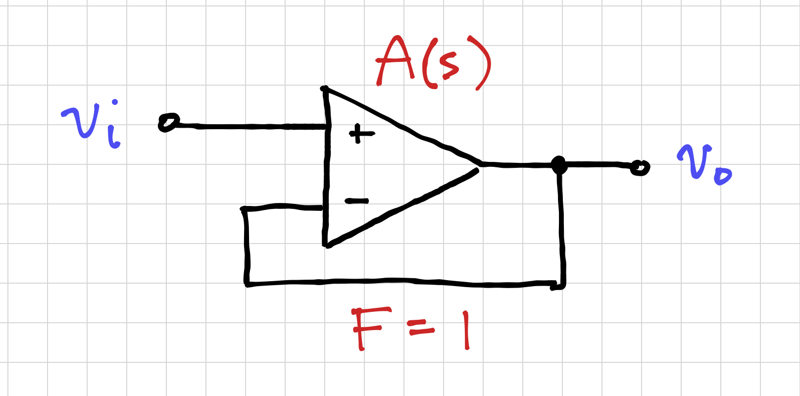
We can build buffers that have relatively large bandwidths by using high-gain amplifiers and placing them in a feedback loop with ![]() , as shown below:
, as shown below:

The closed-loop gain can be written as
![]()
Project Specifications
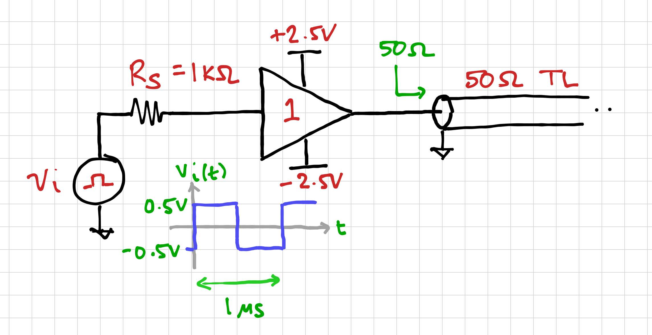
You are tasked to design a buffer that accepts a square wave input voltage with source resistance of ![]() , and drives a
, and drives a ![]() transmission line.
transmission line.

| Supply Voltage | Dual supplies: |
| Output DC Voltage | (same as the input common-mode voltage) |
| Output Load | |
| Gain | |
| Output Waveform | (1) overshoot < 50mV for both rising and falling edges, (2) all oscillations should exponentially decay, and (3) must settle to its final value within 250ns |
| Input Waveform | Square wave with 50% duty-cycle, |
Since (1) the input is differential, (2) a certain amount of gain is needed, and (3) a certain amount of output current is needed to drive the transmission-line load, and the negative input of the forward-gain amplifier, a good place to start is to consider a simple 3-stage amplifier, similar to the amplifier in tutorial 8.
Guide Questions:
- How does the bias current affect the frequency response of the amplifier?
- How much current do you need to drive the output load?
- How much forward gain do you need?
- Will inter-stage amplifier loading be significant?
- What are the dominant poles of
 ? Can you move these poles around? And how does this influence your choice of compensation to ensure stability?
 - Does
 have zeros? Which of these zeros improve or worsen the phase margin?
Simulation Hints:
- When simulating circuits with very large inductors, the simulator may encounter convergence problems, especially during transient simulations. To avoid this problem, you can either add a small series resistance to the inductors, or add the line
.option rseries = 1. This will instruct the simulator to automatically add a 1-Ohm resistor to all your inductors. - It can be advantageous if you think about the structure of your circuit beforehand, and organize it using subcircuits for easier debugging.
- Running an operating point analysis to check the DC biasing of your amplifier before proceeding with other analyses can identify biasing problems early on.
What To Submit:
- A short 2-page writeup of your methodology including:
- An explanation of how you chose your topology, transistor bias currents and the inter-stage DC output voltages within your forward-gain amplifier, together with the calculations used to determine the values of biasing resistors.
- An explanation of how you ensured the stability of your buffer.
- The schematic of your forward-gain amplifier. (not included in the 2-page limit)
- A list of the target and simulated transistor bias currents and amplifier output voltages. (not included in the 2-page limit)
- The DC (quiescent) power consumption of your forward-gain amplifier.
- The DC transfer characteristic of your forward-gain amplifier. (not included in the 2-page limit)
- The DC transfer characteristic of your closed-loop buffer. (not included in the 2-page limit)
- The magnitude and phase response of your loop gain showing the magnitude at low frequencies, the unity-gain frequency, and the phase margin. (not included in the 2-page limit)
- The magnitude and phase response of your closed-loop buffer. (not included in the 2-page limit)
- A transient response plot showing the response of your buffer to a 1V peak-to-peak input square wave (i.e. +0.5V to -0.5V, 50% duty-cycle, 50ns rise- and fall-time, square wave), with a frequency of 1MHz.
- The SPICE netlist you used.
Submissions:
Using your EEE account, submit your report and netlist using this link. Good Luck!
