A Shunt-Feedback Amplifier
Feedback is widely used in amplifiers and other circuits to typically trade-off gain for (1) increased robustness in the face of parameter variations and uncertainty, (2) increased bandwidth, and (3) improved input and output impedances. The cost of feedback, however, includes the possibility of our circuits becoming unstable. Hence we need to make sure that we verify the stability of our feedback circuits.
Analysis of Feedback Amplifiers
Being able to determine the loop gain, ![]() , is key to analyzing the behavior of feedback amplifiers, since
, is key to analyzing the behavior of feedback amplifiers, since ![]() determines (1) the closed-loop amplifier small-signal response, and more importantly, (2) the stability of the amplifier.
determines (1) the closed-loop amplifier small-signal response, and more importantly, (2) the stability of the amplifier.
In the ideal case, we can get the loop gain by simply breaking the loop, as seen in Figure 1, where
![]()
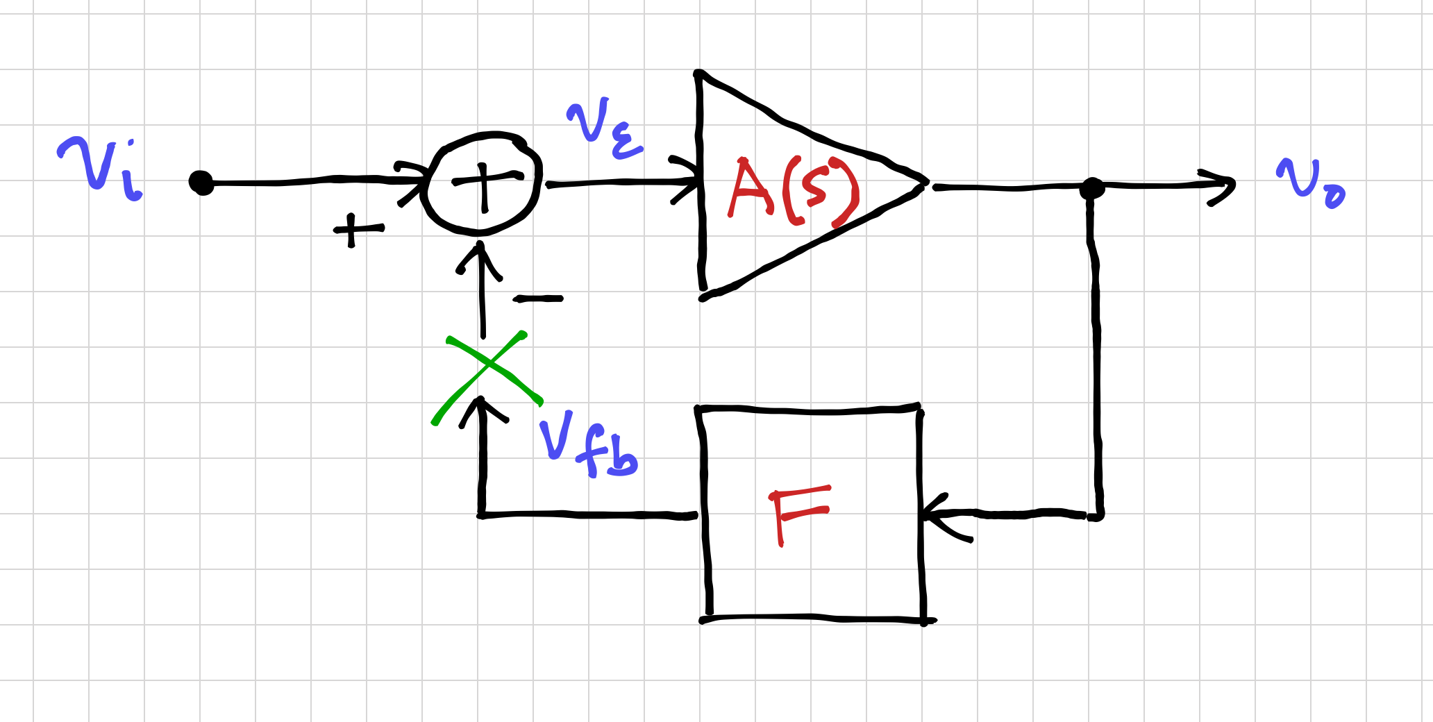
 .
.Then we can easily run a simulation and plot the magnitude and phase of ![]() . However, in most real circuits, breaking the loop to determine the loop gain is not so straightforward. Consider the feedback amplifier in Figure 2.
. However, in most real circuits, breaking the loop to determine the loop gain is not so straightforward. Consider the feedback amplifier in Figure 2.
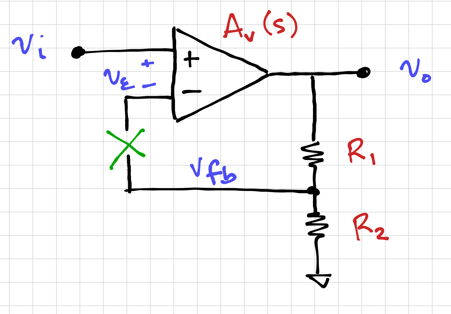
Notice that by breaking the loop, we change (1) the DC bias, both voltage and current, of the negative input terminal of the amplifier, and (2) the AC or small-signal load seen by the feedback circuit. Thus, the resulting circuit can be very different from the one we want to analyze, leading to incorrect loop gain results.
The Loop Gain of a Shunt-Feedback (Shunt-Shunt) Amplifier
Consider a simple shunt-feedback amplifier in Figure 3, using a common-emitter amplifier as the forward gain, and a feedback network composed of the resistor ![]() . Note that this is the same common-emitter amplifier in Figure 1 of tutorial 10, where the two current mirrors are replaced with
. Note that this is the same common-emitter amplifier in Figure 1 of tutorial 10, where the two current mirrors are replaced with ![]() and
and ![]() to simplify the schematic.
to simplify the schematic.
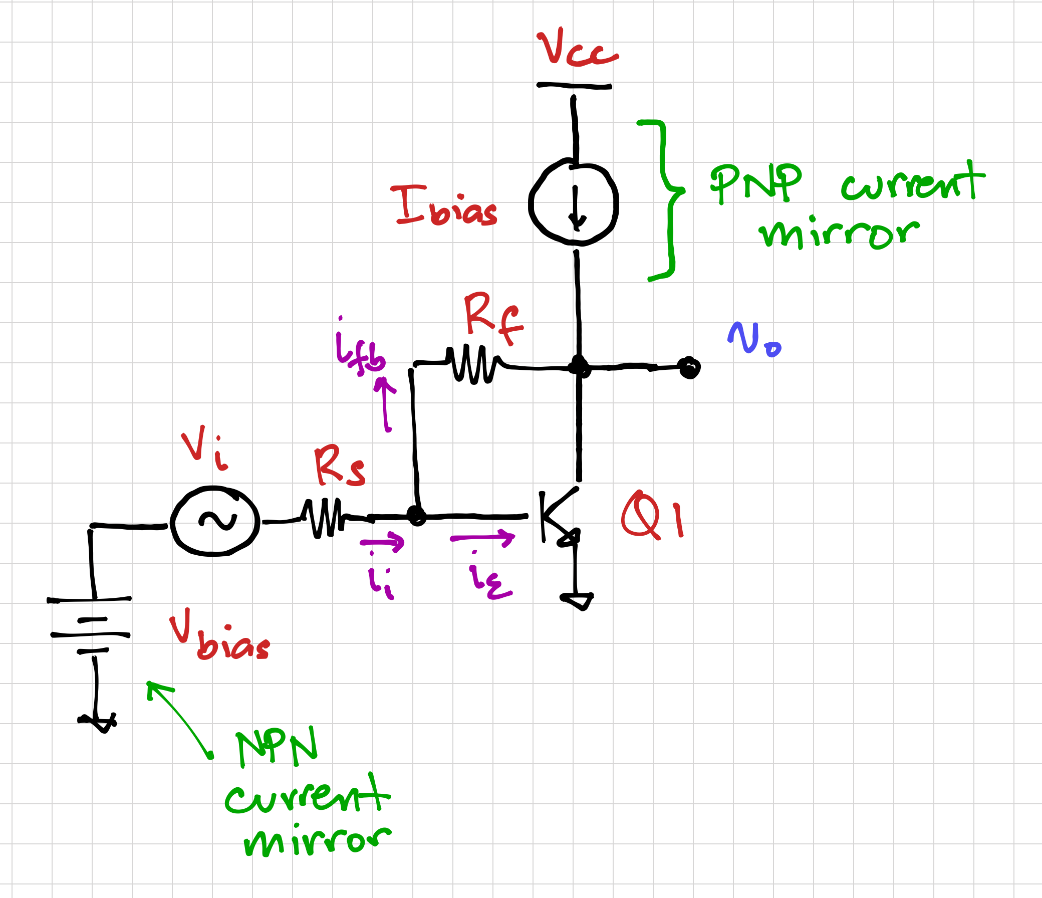
 as the feedback network.
Recall that for a shunt-shunt feedback amplifier, the small-signal input is a current, and the output is a voltage. Thus, the forward gain is
![]()
where ![]() and
and ![]() . The
. The ![]() terms account for the feedback network loading both the input and output of the common-emitter amplifier. Let us ignore
terms account for the feedback network loading both the input and output of the common-emitter amplifier. Let us ignore ![]() for now since the zero is at a relatively high frequency compared to the poles.
for now since the zero is at a relatively high frequency compared to the poles.
The feedback factor is then obtained as
![]()
Thus, we get the (open) loop gain
![]()
From here, we can get the closed-loop gain:
![]()
In order to determine the loop gain via simulation, we need to make sure that (1) the DC bias and (2) the small-signal loading conditions are preserved. One way to accomplish this is to use capacitors and inductors with very large values to selectively pass or block DC signals, and a replica amplifier to ensure correct loading conditions, as shown in Figure 4.
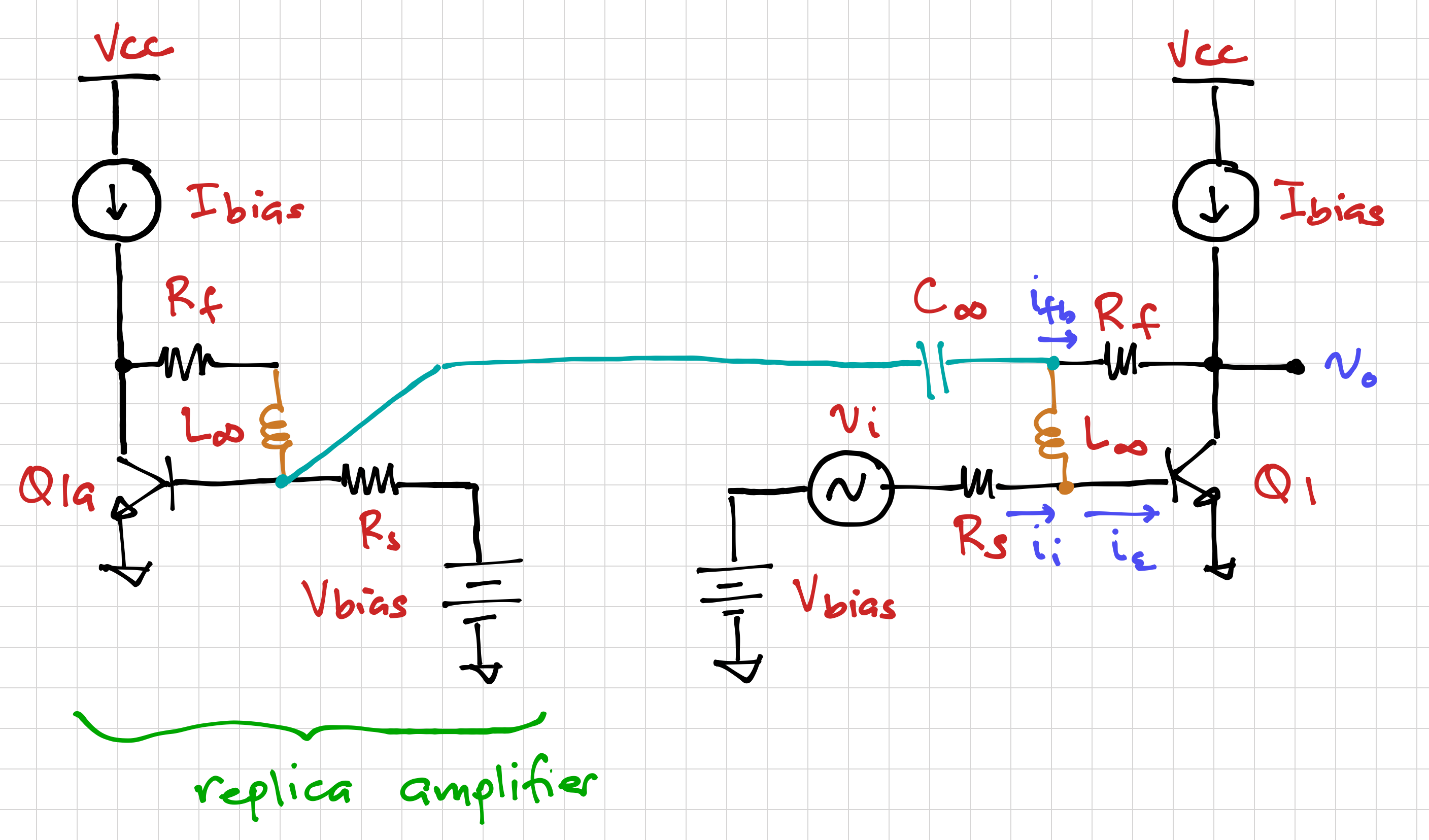
At DC, the two inductors (![]() ) act like short circuits, preserving the bias conditions, and are equivalent to open circuits at any other frequency.
) act like short circuits, preserving the bias conditions, and are equivalent to open circuits at any other frequency.
Similarly, the capacitor, ![]() , is equivalent to an open circuit at DC, isolating the amplifier from the replica. At any other frequency, it acts like a short circuit, presenting the correct load to the feedback network.
, is equivalent to an open circuit at DC, isolating the amplifier from the replica. At any other frequency, it acts like a short circuit, presenting the correct load to the feedback network.
It is important to note that any DC current flowing through the feedback resistor, ![]() , must be supplied by the bias current source,
, must be supplied by the bias current source, ![]() , and must be taken into consideration when designing the bias current source. In this example, however, we can make the resistors relatively large, such that the current through
, and must be taken into consideration when designing the bias current source. In this example, however, we can make the resistors relatively large, such that the current through ![]() is small compared to
is small compared to ![]() .
.
Loop Gain Simulation
Our SPICE netlist contains a description of the common-emitter amplifier subcircuit, instantiated three times: (1) the test amplifier used to obtain the loop gain, (2) the replica amplifier as a load when we break the loop using our large-valued inductor and capacitor, and (3) a closed loop shunt-feedback amplifier used to get the closed-loop response. In this example, ![]() ,
, ![]() ,
, ![]() , and
, and ![]() .
.
We can use this Python script to run an AC analysis to get the magnitude of (1) the forward gain, ![]() , (2) the inverse of the feedback factor,
, (2) the inverse of the feedback factor, ![]() , (3) the loop gain,
, (3) the loop gain, ![]() , and (4) the closed-loop gain,
, and (4) the closed-loop gain, ![]() , as shown below:
, as shown below:
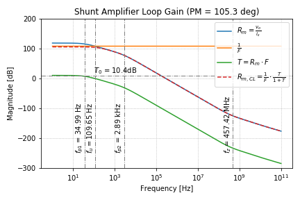
As expected, when ![]() (i.e. 0 dB), or equivalently, when
(i.e. 0 dB), or equivalently, when ![]() , the closed-loop gain becomes
, the closed-loop gain becomes
![]()
and when ![]() (i.e. 0 dB), or
(i.e. 0 dB), or ![]() , we get
, we get
![]()
The unity-gain frequency of the loop gain, ![]() is when
is when ![]() (i.e. 0dB), and marks the boundary between
(i.e. 0dB), and marks the boundary between ![]() and
and ![]() .
.
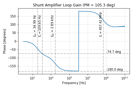
By plotting the phase of the loop gain, we can derive the phase margin of the shunt-feedback amplifier, as shown below:
 .
.We can see that ![]() at the unity gain frequency,
at the unity gain frequency, ![]() . Thus, the phase margin (PM) of the shunt-feedback amplifier is
. Thus, the phase margin (PM) of the shunt-feedback amplifier is
![]()
Thus, we can say that this particular amplifier is stable. It would be a good exercise to see if you can vary the phase margin by varying the locations of the poles and the zero.
Closed-Loop Transient Response
Note that we can easily relate the current input, ![]() , of the shunt-feedback amplifier to the input voltage,
, of the shunt-feedback amplifier to the input voltage, ![]() . Since
. Since
![]()
Then
![]()
Or equivalently
![]()
Thus, for a low-frequency input sinusoid, we can estimate the voltage gain using the value of ![]() from our AC analysis:
from our AC analysis:
![]()
Note that as the magnitude of the loop gain is increased, the closed-loop gain approaches ![]() . This is desirable since the gain can be determined solely by resistor values, and therefore easier to control. What can you do to increase the loop gain?
. This is desirable since the gain can be determined solely by resistor values, and therefore easier to control. What can you do to increase the loop gain?
The plot below shows the simulated closed-loop transient response of the shunt-feedback amplifier, with a 1-Hz input sinusoid.
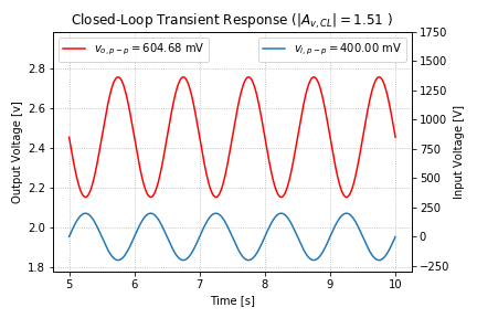
From Figure 7, we can see that the results of our transient simulation are in very good agreement with the results of our AC analysis.
End of Tutorial 11
Congratulations! You have just obtained the loop gain, as well as the closed-loop response of a shunt-feedback amplifier via SPICE, and verified this response using a transient analysis.
