A Two-Stage Amplifier
In many applications, (1) the amplifier gain requirement is larger than the gain a single transistor can provide, and (2) the input and output impedance requirements cannot be met simultaneously by a single amplifier. These gain and impedance requirements usually necessitates the use of multi-stage amplifiers.
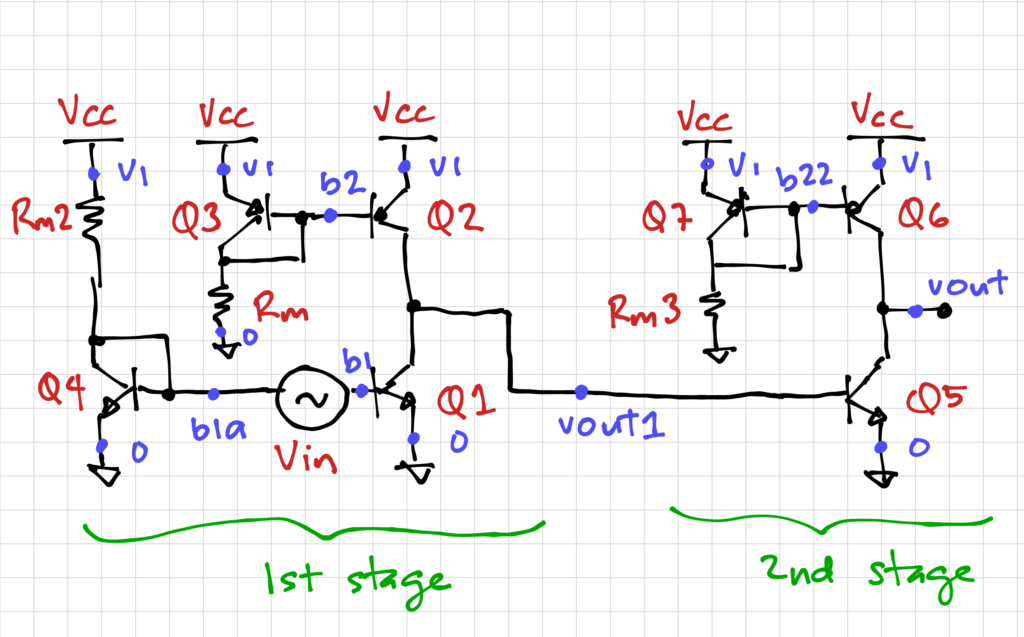
For example, if we need a voltage gain of greater than 5000, we need more than one common-emitter amplifier. Let’s build a 2-stage amplifier composed of two common-emitter amplifiers, as shown below:

We can use the first stage to set the DC input voltage of the second stage. Thus, we need the DC output voltage of first stage to be equal to the DC base-emitter voltage of the second stage:
![]()
Ignoring the effect of ![]() on
on ![]() , we can set
, we can set ![]() , and the DC output voltage of the second stage to
, and the DC output voltage of the second stage to ![]() , we get:
, we get:

Note that ![]() , so transistor
, so transistor Q1 is still in the forward-active region. Then

Note that since ![]() , then
, then ![]() . Thus, we can calculate the value of
. Thus, we can calculate the value of Rm2 as:
![]()
To get the value of Rm, we need ![]() and
and ![]() :
:


Thus,
![]()
Using the same procedure to get Rm3, but with ![]() and
and ![]() , we get:
, we get:

and, similar to tutorial 5,
![]()
We can then create a netlist to describe our 2-stage amplifier:
* Common Emitter Amplifier with Current Mirror Bias
* LPA 2020-04-16

.include 2N390X.lib
.options savecurrents

Vcc		v1	0		dc 5.0

* first stage
* the pnp current mirror
Q2		vout1 b2 v1	2N3906
Q3		b2 b2 v1	2N3906

* the bias resistor
Rm		b2 0		6.312k

* the npn gain transistor
Q1		vout1 b1 0	2N3904

Vin 	b1 b1a		dc 0 sin(0 125u 1k)

* the npn current mirror
Q4		b1a b1a 0	2N3904
Rm2		v1 b1a		4.267k

* second stage
* the pnp current mirror
Q6		vout b22 v1	2N3906
Q7		b22 b22 v1	2N3906

* the bias resistor
Rm3		b22 0		5.277k

* the npn gain transistor
Q5		vout vout1 0	2N3904


.control

dc Vin -0.5m 0.5m 5u
wrdata amp_2stage_transfer_sim.dat v(vout) @Q1[ic] @Q5[ic]

tran 1u 5m
wrdata amp_2stage_transient_sim.dat v(vout) v(b1) v(vout1)

.endc

.end
Using this Python script, we can run the simulation, read-in the data, and plot the results.
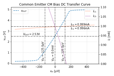
Figure 2 shows the DC transfer characteristics of the 2-stage amplifier. Note that since each common-emitter amplifier is an inverting amplifier, cascading them produces a non-inverting compound amplifier.

Note that we expect a slightly smaller ![]() compared to
compared to ![]() since transistor
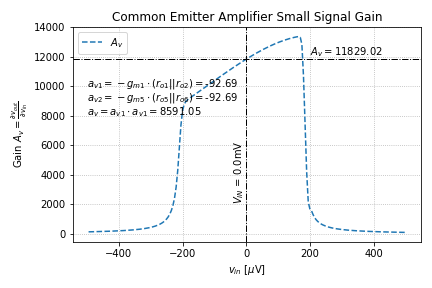
since transistor Q2 is also supplying the base current of transistor Q5. Looking at the x-axis of Figure 2, we can see that the gain is significantly larger than the single-stage amplifier. Figure 3 shows a plot of the small signal gain.

Once again, due to the limitations of the ideal transistor BJT model, we do expect that the errors in our small signal analysis will accumulate as we increase the complexity of our circuit.
Note that we have ignored the effects of the small signal input resistance of the second stage. We can correct for this by re-calculating the small signal gain as:
![]()
If we plug-in our values for ![]() ,
, ![]() , and
, and ![]() , this loading effect reduces the gain by a factor of 0.6. Thus, if we use our simulated values for small signal gain from tutorial 5 (~150 per stage), we get
, this loading effect reduces the gain by a factor of 0.6. Thus, if we use our simulated values for small signal gain from tutorial 5 (~150 per stage), we get ![]() , which is in the same ballpark as our simulation results.
, which is in the same ballpark as our simulation results.
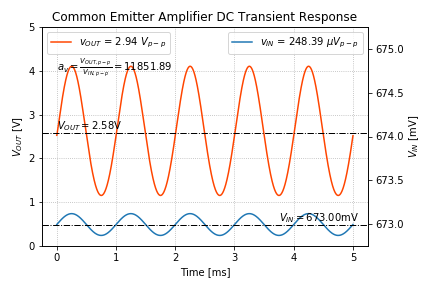
The results of our transient analysis is shown in Figure 4. Again note that the 2-stage amplifier is a non-inverting amplifier.

It turns out we were extremely lucky in biasing our 2-stage amplifier since (1) small changes in the first stage’s DC output voltage can drastically change the transfer characteristics, and (2) the output voltage of the first stage is very sensitive to its input DC voltage.
In real-world amplifiers, we can either control the output voltage precisely using feedback, or we can use circuits that can accept a wide range of input DC voltages, such as differential circuits.
End of Tutorial 6
Congratulations! You have just biased the first and second stage of a 2-stage compound CE-CE amplifier using current mirrors, and examined its small-signal behavior.
