Frequency Response Using ngspice
In the previous tutorials, we were only concerned about the DC characteristics, or what happens when we change the input voltages and currents very slowly. This means that the input frequencies are small enough, that we can treat all capacitors as open circuits, i.e. ![]() , and all inductors as short circuits, i.e.
, and all inductors as short circuits, i.e. ![]() .
.
However, in practice, the signals we are concerned with are time varying signals, which, according to Fourier, can be decomposed into its spectral components, where each component has its own frequency, magnitude, and phase. The goal of our frequency response analysis is to determine the small signal behavior of amplifiers in response to these time varying inputs. And since we are dealing with non-zero frequencies, we cannot treat our capacitors and inductors as open- or short-circuits.
The Transistor Transition Frequency ( )
)
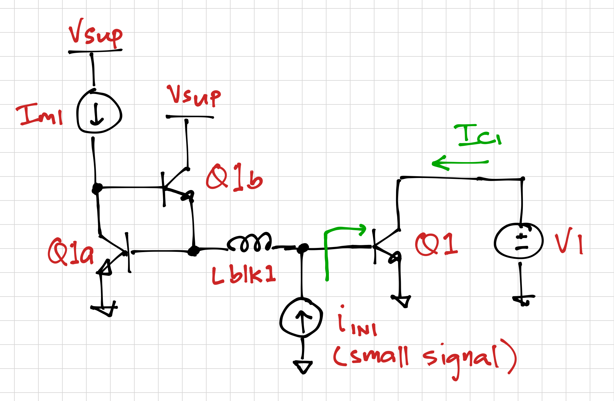
Before we look at the frequency response of amplifiers, let us examine the effects of time varying inputs on a BJT. Consider the circuit below:

 .
.Note that, once again, we are using transistors Q1a and Q1b to generate ![]() to get
to get ![]() . We then use
. We then use V1 to set ![]() to a reasonable value, ensuring that the transistor is in the forward-active region.
to a reasonable value, ensuring that the transistor is in the forward-active region.
Let us add a small signal input, ![]() , and let us see how the transistor behaves as we increase the frequency of the small signal input current. Note that we are using a large blocking inductor,
, and let us see how the transistor behaves as we increase the frequency of the small signal input current. Note that we are using a large blocking inductor, ![]() , to prevent the small-signal current from going into the bias circuit because we want all of this input current going into the base of
, to prevent the small-signal current from going into the bias circuit because we want all of this input current going into the base of Q1, but we also want the DC bias current and voltage to get to the base of Q1.
If we inject a low-frequency small-signal current into the base of Q1, we expect a small signal collector current equal to:
![]()
As we increase the frequency of the small-signal input current, the transistor parasitic capacitances cannot be ignored any longer. The largest of these capacitances are (1) the base-emitter capacitance, composed of the base-emitter junction capacitance and the base charging capacitance, ![]() , and (2) the collector-base junction capacitance,
, and (2) the collector-base junction capacitance, ![]() .
.
Thus, our expression for the small-signal collector current becomes:
![]()
Notice that at high input frequencies, the impedances of the two capacitors become significantly smaller than ![]() . At this point, the voltage
. At this point, the voltage ![]() also becomes smaller, resulting in a smaller small-signal collector current, making it seem that the transistor
also becomes smaller, resulting in a smaller small-signal collector current, making it seem that the transistor ![]() is decreasing as well.
is decreasing as well.
For a transistor to amplify an input signal, it has to have a current gain
![]()
So one useful metric is to figure out the frequency at which the small-signal current gain is equal to 1. This is the transistor’s transition frequency. Note that since the collector of Q1 is at small-signal ground, it is also called the short-circuit current gain. Thus
![]()
We can then express the transition frequency as:
![]()
Simulating 
Let’s use this SPICE netlist to determine the transition frequency of the 2N3904 NPN bipolar transistor.
* Transistor transition frequency
* LPA 2020-04-16

.include 2N390X.lib

.options savecurrents

* the npn 2N3904 transistor
Q1		c1 b1 0		2N3904

Iin1 	b1 0		dc 0 ac 1
Lblk1	b1a b1		1k

* the npn current mirror
Q1a		c1x b1a 0		2N3904
Q1b		vcc c1x b1a		2N3904
Im1		vcc c1x		0.9m
V1		c1 0 		dc 2.5

Vsup	vcc 0 		dc 2.5

.control

op
let ft_2n3904_sim = '@Q1[gm]/(2*3.14*(@Q1[cpi]+@Q1[cmu]))'
print @Q1[ic] @Q1[gm] @Q1[cpi] @Q1[cmu] ft_2n3904_sim

ac dec 1000 100k 10G
wrdata bjt_2n3904_ft_1mA_sim.dat i(V1)

let mag_iV1 = abs(i(V1))
meas ac ft_2n3904 when mag_iV1=1

alter Im1 = 9m

op
let ft_2n3904_sim = '@Q1[gm]/(2*3.14*(@Q1[cpi]+@Q1[cmu]))'
print @Q1[ic] @Q1[gm] @Q1[cpi] @Q1[cmu] ft_2n3904_sim

ac dec 1000 100k 10G
wrdata bjt_2n3904_ft_10mA_sim.dat i(V1)

let mag_iV1 = abs(i(V1))
meas ac ft_2n3904 when mag_iV1=1

.endc

.end
We add another input source specification, the ‘ac‘ magnitude, as seen in line 11, when we describe the source Iin1. Since the AC analysis is a small-signal analysis, i.e. it calculates the small-signal equivalent circuit from the bias voltages and currents, it is a linear analysis. Thus, if we assign the input a value of 1A, the resulting collector current value will be the same as the current gain.
To specify the AC analysis, we use the ac command in lines 28 and 40, with the format ac dec <nd> <fstart> <fstop>, where nd is the number of points per decade. the simulator then calculates the small signal response of the circuit from frequency fstart to frequency fstop. Note that the node voltages and currents are phasors (complex numbers).
We use the measure or meas command in lines 31, 32, 43, and 44 to find the frequency when the magnitude of the current through the voltage source V1 is equal to 1. Thus this frequency is the transition frequency of the BJT.
To calculate the transition frequency, we can also use the bias voltages and currents to calculate ![]() ,
, ![]() , and
, and ![]() , as shown in lines 25 and 37.
, as shown in lines 25 and 37.
Let’s simulate this circuit for two values of collector currents: 1mA and 10mA. We can use the alter command in line 34 to change the bias current. Running the simulation results in the following report:
******
** ngspice-31 : Circuit level simulation program
** The U. C. Berkeley CAD Group
** Copyright 1985-1994, Regents of the University of California.
** Please get your ngspice manual from http://ngspice.sourceforge.net/docs.html
** Please file your bug-reports at http://ngspice.sourceforge.net/bugrep.html
******
ngspice 1 -> source bjt_2n3904_ft.sp

Circuit: * transistor transition frequency

Doing analysis at TEMP = 27.000000 and TNOM = 27.000000


No. of Data Rows : 1
@q1[ic] = 1.048843e-03
@q1[gm] = 3.474254e-02
@q1[cpi] = 2.246856e-11
@q1[cmu] = 1.990019e-12
ft_2n3904_sim = 2.261886e+08
Doing analysis at TEMP = 27.000000 and TNOM = 27.000000


No. of Data Rows : 5001
ft_2n3904           =  2.219428e+08
Doing analysis at TEMP = 27.000000 and TNOM = 27.000000


No. of Data Rows : 1
@q1[ic] = 1.027438e-02
@q1[gm] = 2.636559e-01
@q1[cpi] = 1.150564e-10
@q1[cmu] = 2.011312e-12
ft_2n3904_sim = 3.586252e+08
Doing analysis at TEMP = 27.000000 and TNOM = 27.000000

 Reference value :  1.60325e+08
No. of Data Rows : 5001
ft_2n3904           =  3.554370e+08
ngspice 2 ->
From the simulation results, we can see that both the AC analysis and operating point analysis will give about the same value:
| Bias current | Transition Frequency |
| 1 mA | 221.94 MHz |
| 10 mA | 355.44 MHz |
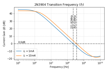
Using this Python script, we can plot the results of the AC analysis, as shown below:

Note that if we want to maintain the inherent gain of our transistors, we should operate well below the transition frequency, e.g. 1 to 2 decades below ![]() . We also observe that
. We also observe that ![]() is dependent on the DC collector current. In most cases, it is the frequency response requirements that determine the required bias currents.
is dependent on the DC collector current. In most cases, it is the frequency response requirements that determine the required bias currents.
End of Tutorial 9
Congratulations! You have just performed a SPICE AC analysis to determine the transition frequency, ![]() of the 2N3904 BJT.
of the 2N3904 BJT.
